


Root Cause Analysis for Contamination Defects
In semiconductor manufacturing, contamination defects significantly impact quality and reliability. Factors such as raw materials, methods, machines, environment, and personnel contribute to these defects. Utilizing AI-driven root cause analysis (RCA) tools, like ProSolvr, enables manufacturers to effectively identify and mitigate contamination sources, thereby enhancing operational excellence and ensuring high-quality standards.
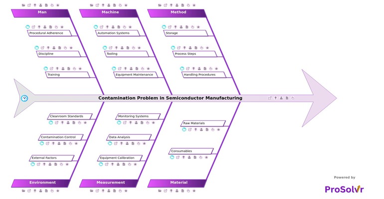
Visual root cause analysis is essential in addressing contamination defects. This technique allows teams to quickly pinpoint issues such as impurities in silicon wafers, inadequate cleaning protocols, and improper storage conditions. By visually mapping out the causes, immediate problem-solving is facilitated, and long-term improvements are supported through Corrective and Preventive Actions (CAPA). Tools like ProSolvr enhance this process, promoting team collaboration and efficiency, and ultimately improving overall quality and reliability.
The integration of Six Sigma methodologies with AI-driven RCA tools can substantially reduce contamination defects in semiconductor manufacturing. Six Sigma focuses on process improvement and variability reduction, while AI-driven tools provide deep data insights for comprehensive analysis. This synergy helps organizations achieve higher precision and control over their manufacturing processes. ProSolvr aids these efforts by offering advanced capabilities for implementing and sustaining improvements, driving operational excellence.
Boosting team efficiency and collaboration is crucial for combating contamination defects. With ProSolvr, the visual root cause analysis tool, teams can accurately and swiftly identify the root causes of contamination, leading to faster resolution times and a reduction in recurring issues. Solutions like ProSolvr empower teams with the insights and tools necessary to perform optimally, ensuring continuous improvement and operational excellence.
In conclusion, addressing contamination defects in semiconductor manufacturing requires advanced root cause analysis (RCA) tools for effective resolution. By leveraging AI-driven RCA, visual root cause analysis, and methodologies like Six Sigma, companies can significantly enhance quality, reliability, and overall operational performance. ProSolvr stands out as a robust solution supporting these goals, helping teams collaborate more effectively and achieve higher levels of efficiency and excellence.
Minimizing contamination defects in semiconductor manufacturing is crucial for enhancing product quality and operational efficiency. Utilizing AI-driven root cause analysis (RCA) tools like ProSolvr allows teams to swiftly identify and mitigate contamination sources. Integrating visual RCA and Six Sigma methodologies fosters continuous improvement, regulatory compliance, and team collaboration, driving operational excellence and reliability.
Who should use the Contamination Defect in Semiconductor Manufacturing template?
The Contamination Defect in Semiconductor Manufacturing template is typically used by semiconductor manufacturing engineers, quality assurance personnel, or process engineers involved in identifying, analyzing, and resolving contamination issues in semiconductor fabrication processes. This template helps in documenting:
- Defect Details:
- Description of contamination issue (e.g., particle size, type, location)
- Measurements and characteristics of the contamination
- Impact Assessment:
- Evaluation of the contamination's impact on process, product quality, and yield
- Quantification of potential losses (e.g., yield loss, rework)
- Root Cause Analysis:
- Investigation into the root cause of contamination
- Examination of equipment, materials, handling procedures, and environmental factors
- Corrective Actions:
- Proposed actions to mitigate or eliminate contamination
- Implementation plan for corrective measures
- Verification and Validation:
- Confirmation of the effectiveness of implemented actions
- Testing, monitoring, or further analysis to ensure sustained improvement
Overall, the Manufacturing Defects template serves as a structured tool to help organizations in the manufacturing industry enhance quality, efficiency, compliance, and operational excellence.
Why use the Contamination Defect in Semiconductor Manufacturing template?
The Contamination Defect in Semiconductor Manufacturing template is used for several important reasons, which include:
- Structured Problem Solving: Provides a systematic approach to identify, analyze, and resolve contamination issues in semiconductor manufacturing processes.
- Documentation: Formalizes the recording of contamination defect details, impact assessment, and corrective actions, ensuring clarity and traceability.
- Root Cause Analysis: Facilitates thorough investigation into the root causes of contamination, enabling effective corrective and preventive actions.
- Quality Improvement: Supports continuous improvement initiatives by addressing contamination defects, leading to enhanced product quality and process efficiency.
- Communication and Collaboration: Serves as a communication tool among stakeholders, promoting better collaboration and informed decision-making.
- Risk Mitigation: Reduces the risk of yield losses, production delays, and customer dissatisfaction by addressing contamination issues promptly and effectively.
- Regulatory Compliance: Ensures compliance with regulatory standards by documenting contamination issues and their resolutions for audit and quality management purposes.
Overall, the Contamination Defect in Semiconductor Manufacturing template ensures that contamination issues are not only addressed promptly but also systematically analyzed to prevent their recurrence, thereby contributing to improved manufacturing efficiency and product reliability.

